- Menu Close
-
Healthcare
- Overview
- Industries
- Regulatory services
Regulatory services
Regulatory services for healthcare companies
- Performance Materials
-
Technology
- Overview
- Industries
- DKSH Philippines products
Our products
Search our product database.
-
Services
- Overview
- Sourcing
Sourcing
Accessing a global sourcing network.
- Market insights
Market insights
Generating ideas for growth.
- Marketing and sales
Marketing and sales
Opening up new revenue opportunities.
- Distribution and logistics
Distribution and logistics
Delivering what you need, when you need it, where you need it.
- After-sales services
After-sales services
Servicing throughout the entire lifespan of your product.
- Insights
- Home
- Technology
- DKSH Philippines products
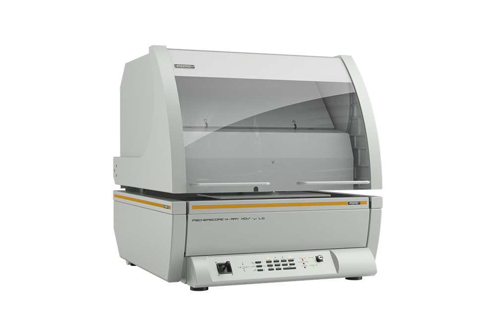
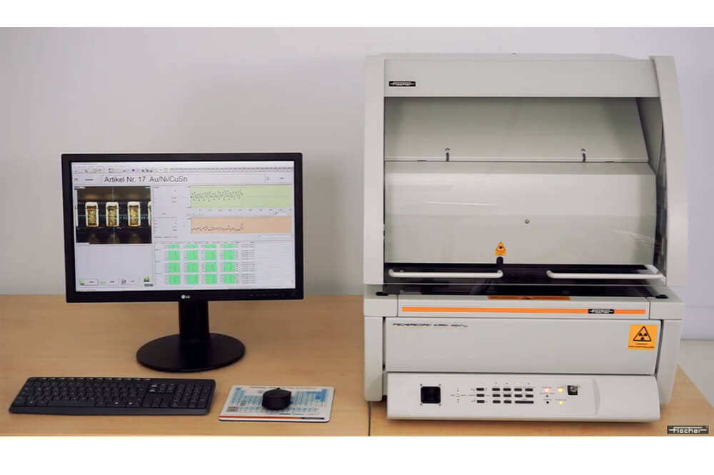
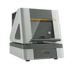
- Helmut Fischer – Fischerscope X-ray XDV-µ
- Home
- Technology
- DKSH Philippines products
- Helmut Fischer – Fischerscope X-ray XDV-µ